
2025-04-20: More Hardware updates
These last few weeks have been busy. Busy with life in general, but also busy with validating the EV1 revision of the APEC SoM. All in all, the validation has been a tremendous success. Thus far I’ve validated most “realistic” use cases, and the issues I’ve found have been fairly minor. In this post I’ll dig a little deeper into the issues, and go in to what the plan for the APEC SoM is.
EV1 issues
ESP32-C6 control over RP2350 EN and Bootsel
One of the nice features of the board is that the ESP32-C6 can reboot the RP2350. It does this by controlling N-channel FETs that can pull the EN and Bootsel pins of the RP2350 low. In order to prevent undefined behavior when the ESP32-C6 is resetting and what-not, there are pull-downs on the gate, specifically 10K pull-downs (it’s a nice, pretty weak pull-down value).
Sadly, I didn’t read the ESP32-C6 data sheet closely enough, and picked pins that have a weak pull-up at reset. That weak pull-up means that at reset the voltage at the gate is around 700 mV, which - for the particular FET I’m using - is above the \(V_{gs(th)}\).
This can be remedied in different ways. Either I can pick different pins on the ESP32-C6, which don’t have WPU at reset, or I can change the pull-downs or FETs. Purely out of convenience, I’m leaning towards changing the pull-downs (to 1K5). Picking different pins would both mean a substantial rerouting, and it would mean that the EV1 revision and the future EV2 revision would need different firmware versions. Also, replacing the resistors is theoretically possible on the EV1 board (although they are 0201 sized, so a microscope and a steady hand is definitely needed), so I can actually test the values before ordering a new revision.
Power supply sequencing when \(V_{in} < 6V\)
The APEC SoM uses power supply sequencing. This is because while the RP2350 have (some) 5V tolerant pins, they are only 5V tolerant when IOVDD = 3.3V. In the EV1, the sequencing is a follows: 3.3V -> 6V -> 5V, 5VA. This ensures the 5V supply is only turned on after the 3.3V supply is stable. The result is that if you’re powering your 5V peripheral from the on-board LDO, you won’t be able to put 5V into the RP2350 when IOVDD < 3.3V.
So far, so good, right? Well, yes, but also no. If you’re powering the APEC SoM through USB, \(V_{in}\) will be 5V. This means that the 6V domain will never be considered stable, and as such the 5V and 5VA domain will never enable. Is this a big deal? No, not really, the recommended \(V_{in}\) is 9-12V. That being said, it’s nice (for testing and firmware development) to be able to have the ADS124S08 ADC powered when powering just over USB.
I’m leaning towards sequencing the power supplies as follows: 3.3V -> 6V, 5V, 5VA. It’s technically worse, but in practice it will mean that when \(V_{in} = 5V\), the 5V and 5VA rails will be powered but at around 4.5V. This is adequate for development and debugging.
What’s left to validate?
As I said, most of the “realistic” use cases have been validated, but some validation remains.
- RP2350 ADC Performance - Thus far I’ve only used the ADC capable pins for digital IO
- RP2350 HSTX Performance - I may or may not be able to do this. The HSTX peripheral works but I might need access to a better oscilloscope to actually verify that there isn’t too much cross-talk at higher speeds. Another option would be to actually use the HSTX peripheral for something.
- ESP32-C6 -> RP2350 UART Boot - I’ve wired the ESP32-C6 so that it can use the RP2350 UART Bootloader for recovering from a bad flash. I have been able to verify communications, but I haven’t tried to upload a binary yet.
- ADS124S08 Performance - I’ve validated communications, but I still need to perform some actual measurements and do some performance characterization
- ESP32-C6 JTAG - I’ve only used the on-board USB JTAG controller, not the actual pins.
- FDC1004 parasitic capacitance - On the debug board I have around 2 pF of parasitic capacitance (when using Flexypins). I also want to validate the parasitic capacitance of just the module.
- DC-DC Temperature tests at full load - The TPS82130 is able to source 3A, which is a lot of current, I want to make sure that it doesn’t get too hot.
- EMI pre-pre-compliance testing - I do have a cheap spectrum analyzer and some near-field probes. By no means enough to do compliance testing, or even pre-compliance testing, but enough to do pre-pre-compliance testing
What’s next?
As you might remember, I mentioned an EV2 revision earlier. That is the next step for the actual SoM, but not the most immediate next step for me. Considering the relatively few issues with the EV1 revision, I’m doing a couple of boards in between.
Dev rig carrier
First up is a carrier board for my dev rig.
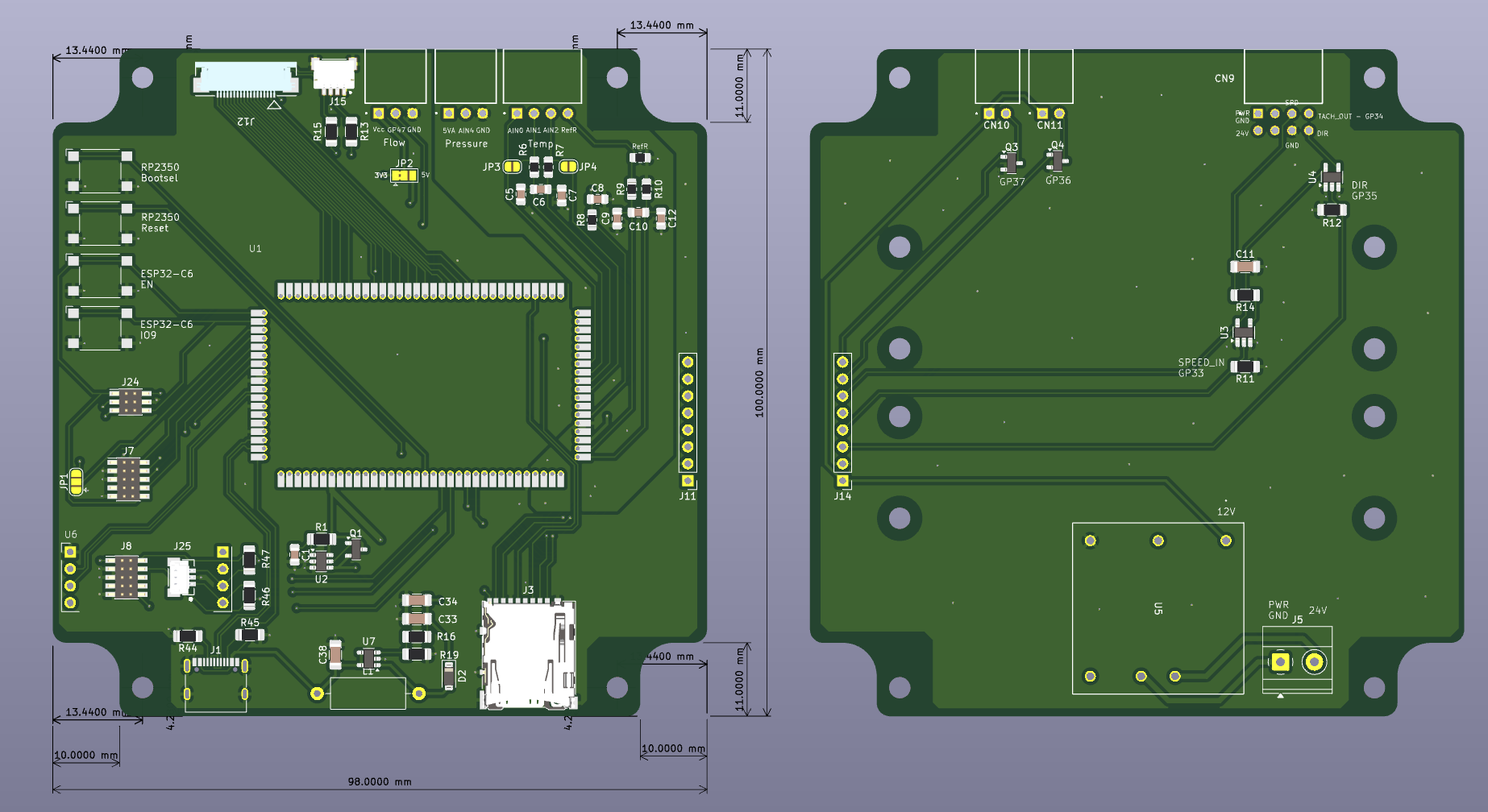
This board (or rather these boards) is meant to fit inside of a Hammond Manufacturing 1593W enclosure. It basically just has the IO I need for my dev rig, and some other niceties to make development easier. The best part is that it’s all hand solderable, mosty 1206 and 0805 (although the USB port and the EyeSPI connector are pretty fine pitch). This allowed me to do the assembly myself, so getting five of each PCB was $9. Of course, I’ll also need components, but a lot of the components are pretty standard, and I already have most of them from other projects.
Features
- EyeSPI connector
- QWIIC connector
- USB-C connector
- MicroSD card reader (connected over a 4 bit bus)
- Filters and reference resistor for one PT100 RTD
- Filters and reference for an analog pressure transducer
- Flow sensor connector
- Gear pump connector
- Connectors for two SSRs (controlling the boiler and three way solenoid)
- 24V-12V step-down
- LM5050-1 OR-ing controller allowing both USB and 24V input at the same time
- Boost converter to step up USB \(V_{in}\) to 12V
- ESP-Debug headers
- Three different RP2350 debug headers
- 10 pin ARM Cortex
- Raspberry Pi Debug header
- Femtoprobe
I know what you’re thinking. “What’s a Femtoprobe?”
Femtoprobe
One of the things I like about the ESP32-C6 (and the ESP32-S3) is that it has a built-in USB JTAG interface. The RP2350 does not, so you’ll need something like a Raspberry Pi Debug Probe or a J-Link to debug it, which is fine. The APEC SoM does however have a USB hub with 2 extra channels, which got me thinking. Why not make a smaller version of the Debug Probe, that connects using a pin header instead of a USB connector? The Raspberry Pi Debug Probe is pretty small, but my probe is smaller, and as such, I’m calling it the Femtoprobe.
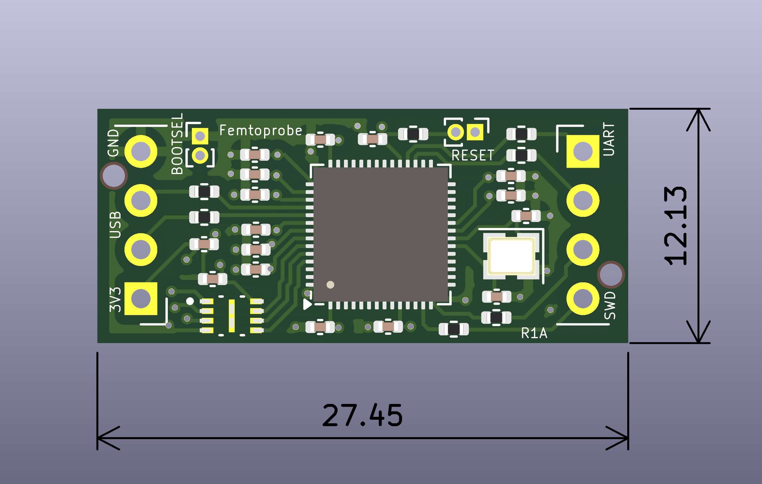
Measuring just 27.45 mm by 12.13 mm, it’s really tiny. It’s not as fancy as the Raspberry Pi Debug Probe, and it’s way less fancy than a J-Link, but it is a lot smaller.
The Femtoprobe is intended to be plugged in using a pin header, so keep it connected when you’re using it, remove it when you don’t need it. In the case of the Dev rig carrier, that means I can do all firmware development using just a single USB-C cable.
APEC SoM EV2
I am planning to order a second Engineering Verification batch of the APEC SoM in a couple of months (aptly named EV2). This will be a larger run, preliminarily 20 boards. I am planning to distribute some of these boards as engineering samples (some for free, some at cost), so if you are interested in making use of the APEC SoM in a project, get in touch.
The boards are engineering samples, meaning they’re not for resale or use in a final product, and may only be used for development, testing or evaluation purposes. It doesn’t come with any form of certifications (nor the documentation necessary to certify anything using it), nor any warranties of any kind. Furthermore, the APEC SoM is a part requiring integration, targeting professional users.
Bianca with Gear Pump Carrier
At some point I will be ordering a carrier for my Bianca, which I’ll then install a gear pump into. At this point, I don’t know if this will be before or after ordering the EV2 run. The design, however, is fairly finalized.
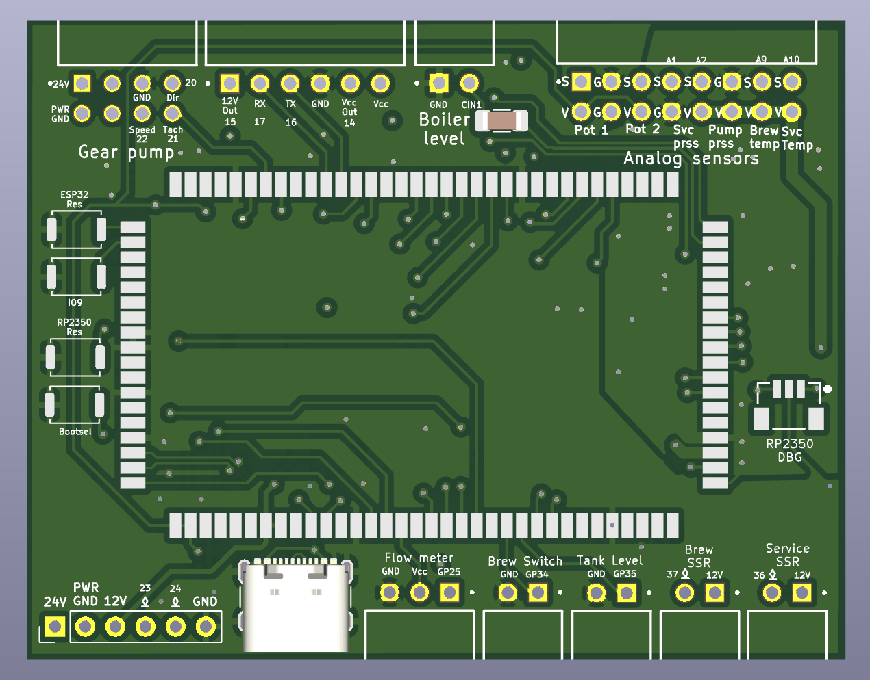
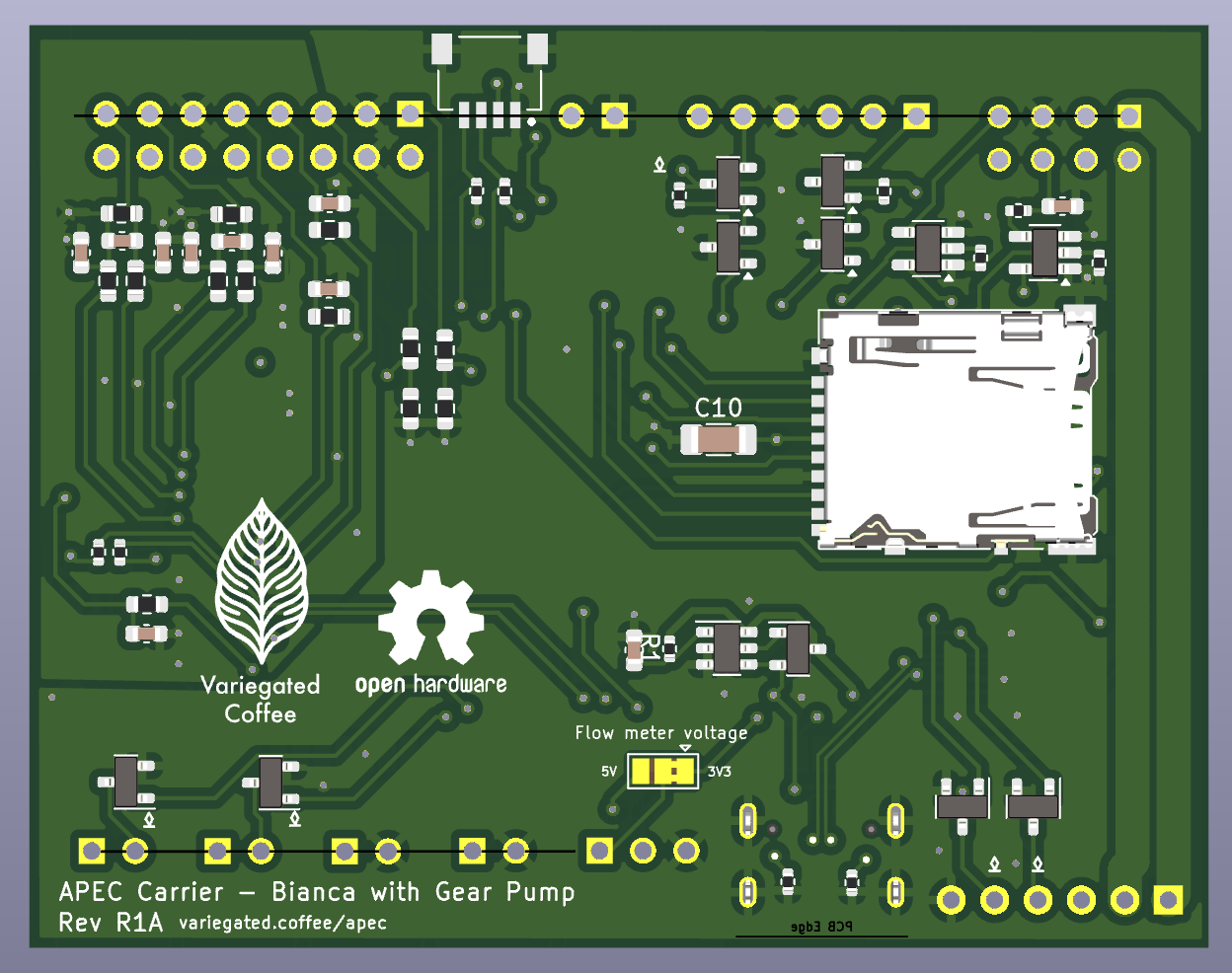
This board is absolutely more compact than the Dev rig carrier, and it shows. That being said, I may be able to pick components large enough to hand solder here too. Some footprints will be 0603, but even that is pretty doable.
Features
- USB-C connector
- QWIIC connector
- MicroSD card reader (connected over a 4 bit bus)
- Filters and reference resistor for two NTC thermistor
- Filters and reference for two analog pressure transducers
- Connector for two potentiometers
- Flow sensor connector
- Gear pump connector
- LCC connector
- Connectors for two SSRs (controlling the brew boiler and steam boiler)
- LM5050-1 OR-ing controller allowing both USB and 12V input at the same time
- Raspberry Pi Debug header (no room for a Femtoprobe)
I’ve also created a corresponding HV board with two mechanical relays and a 24V-12V step-down
Closing words
As always, if you have any thoughts or comments, I’m available on the Discord, and I love to hear what you think.